Tools
– Photoshop ($10/month)
– Eagle Cad (free)
– Inkscape (free)
Introduction
If you are someone who likes to create custom PBC’s and uses Eagle Cad, but find it difficult to create custom shapes and designs this tutorial is for you.
I have seen other tutorials doing this with KiCad EDA and Inkscape, but since lots of people use Eagle Cad, I set out to make a simple demo on creating custom board shapes for Eagle Cad.
Side note
I like Eagle Cad over KiCad is because it feels way more stable and professional, and best of all it integrates with Fusion 360 enabling me to quickly 3D model my PCB’s, make cases and renderings of the end product.
Step One Photoshop
NOTE: You can do this part with Inkscape if you’re more proficient with it, or any other graphics tool that will allow you to save out PNG files.
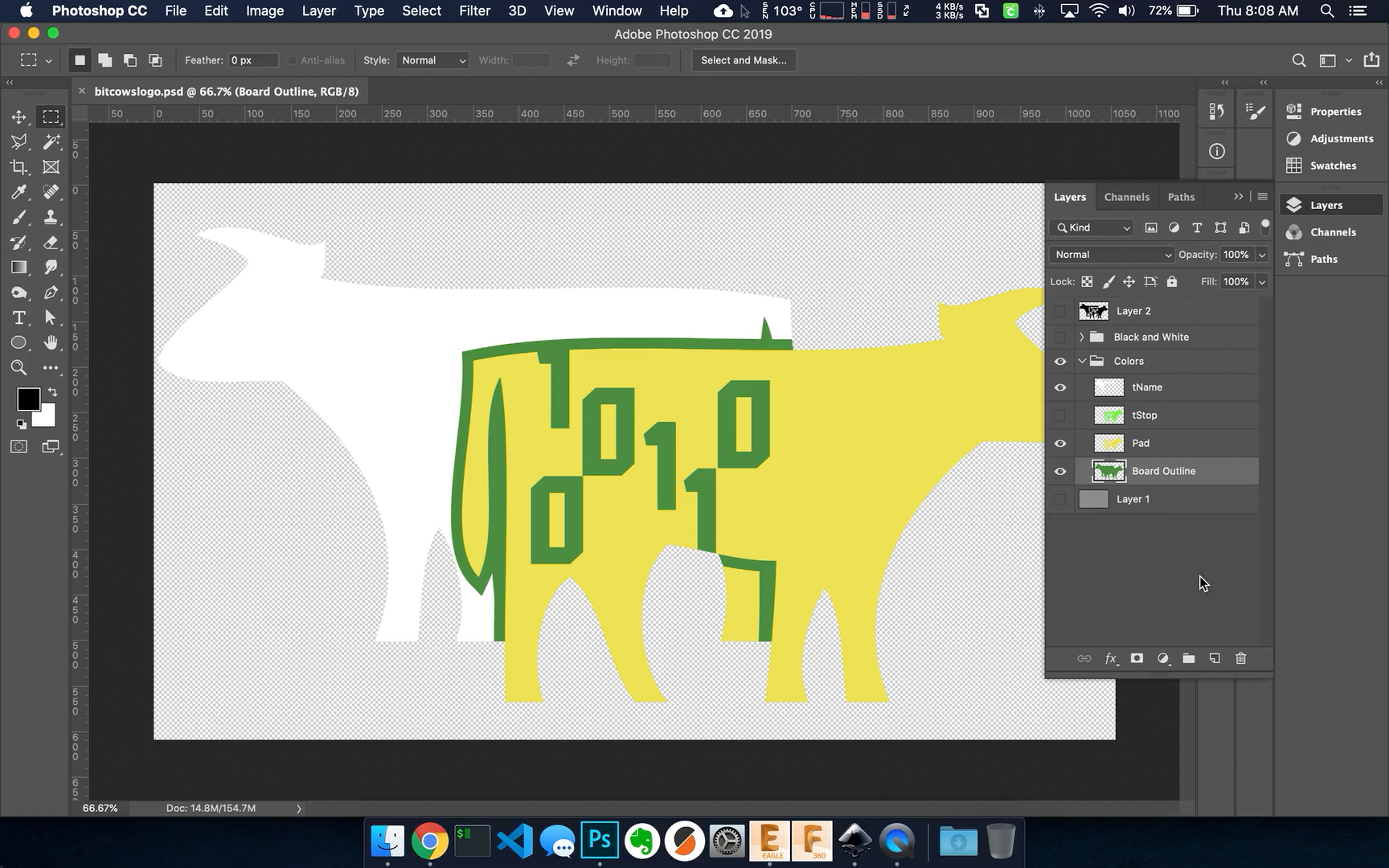
To begin you will need to identify what you want to create. A few things to keep in mind are it needs to be something that can be cut out of FR4 fiberglass so spiderwebs and tiny threads might not work. Also, it needs to be something that you can convert into about 4 colors. Rainbows and Kaleidoscopes might not be the best choice here either. So for this example I choose my logo. I’m making it so that there is copper showing through and a screen print over the solder mask.
To begin with I broke my logo into 4 pieces.
- Board outline (Dimension)
- Copper layer (Pad)
- Solder mask Stop layer (tStop)
- Screen print layer (tName)
To make my life easy I named each layer the name of the Eagle Cad layer (tStop, tName, Pad, Dimension). This way when I save the file I know what im working with.
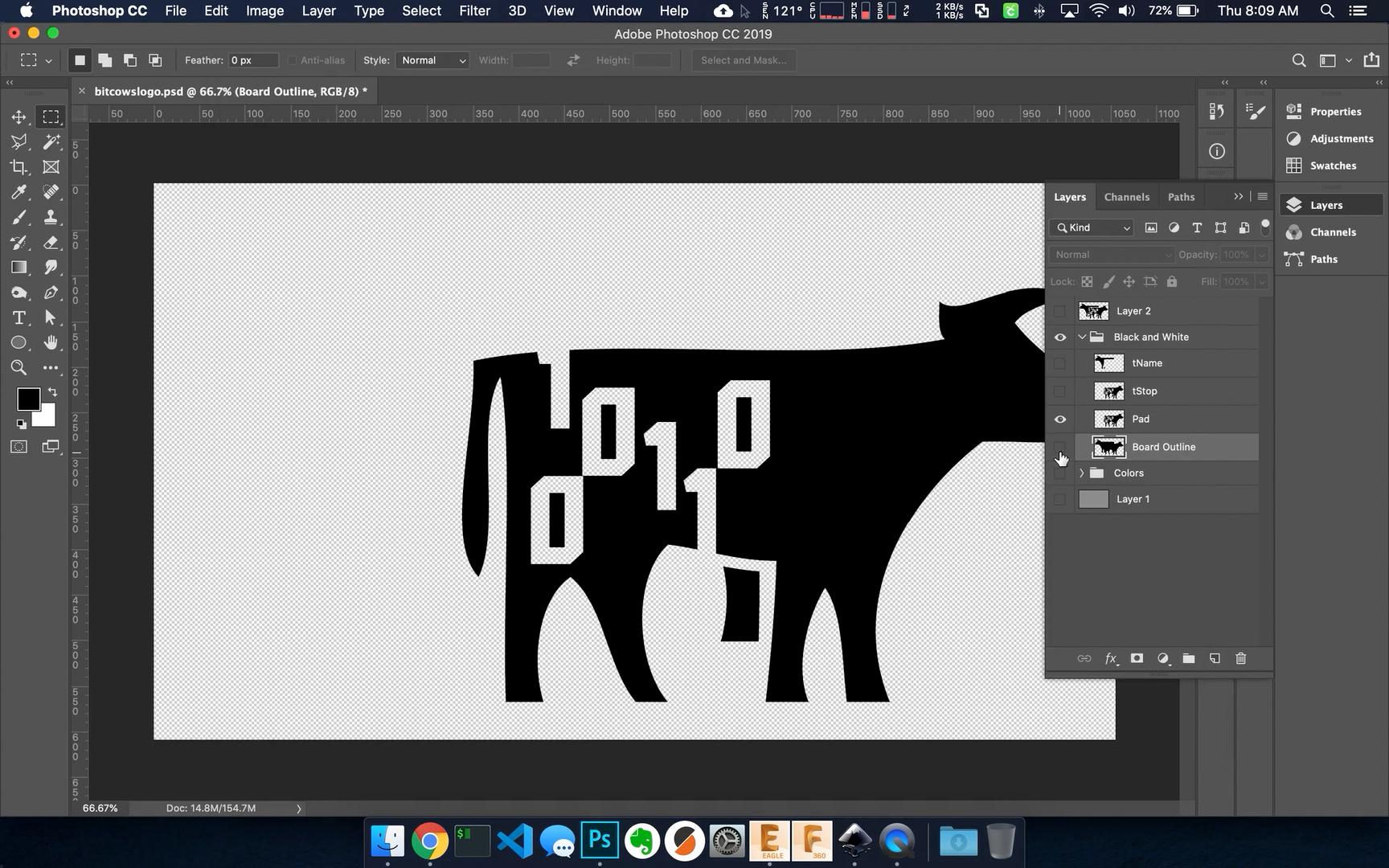
Once you have that laid out you should convert all the layers to simple black. The reason for this is so Inkscape can trace it easily. Save each layer as a png and name them the same as the layers. (tStop.png, tName.png, Pad.png, Dimension.png)
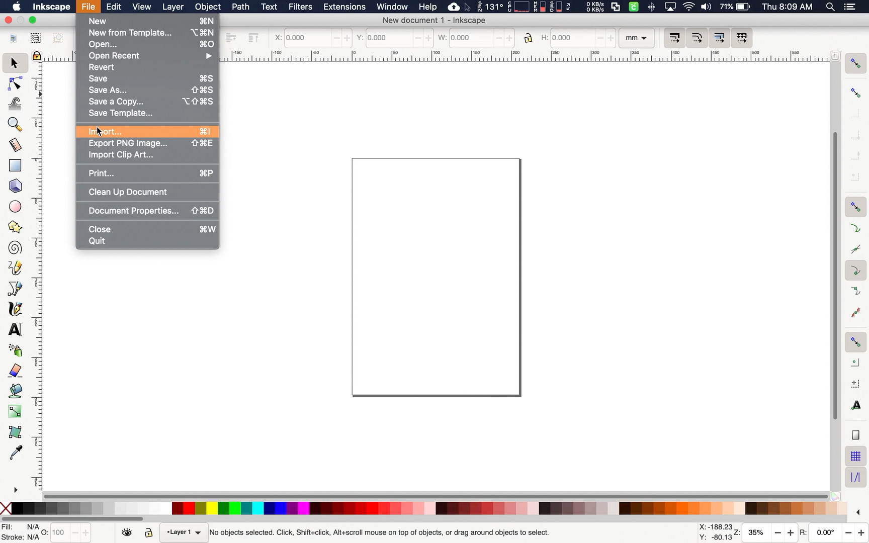
Step Two Inkscape
After they are all saved out we can open up Inkscape by importing them (Menu Item: File > Import...).
Next you will change the size to the appropriate size and location using the highlighted fields. Make sure you click the lock button and adjust either the width or the height. Then place them at the lower left corner of the page. This ensures your layers will all line up correctly in Eagle Cad.

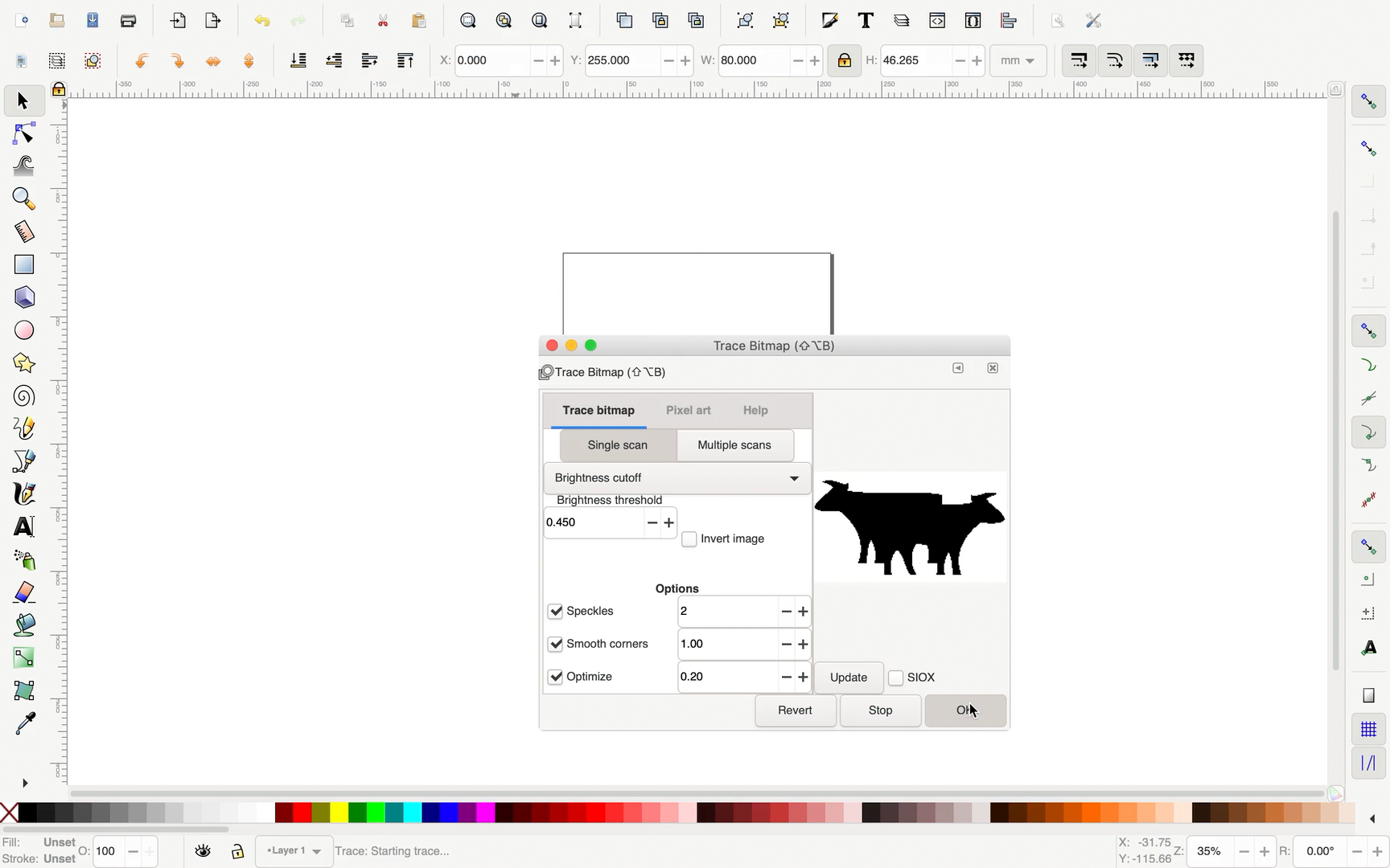
Next you will need to convert all your pngs to paths using the Trace Bitmap (Menu Item: Path > Trace Bitmap..)
Lastly save your file in the SVG format (default)
Step Three SVG Converter
Now its time to convert your SVG into code that Eagle Cad can ingest. By going to djmason9.github.io you can convert your SVG file to Eagle scripts for creating your PCB.
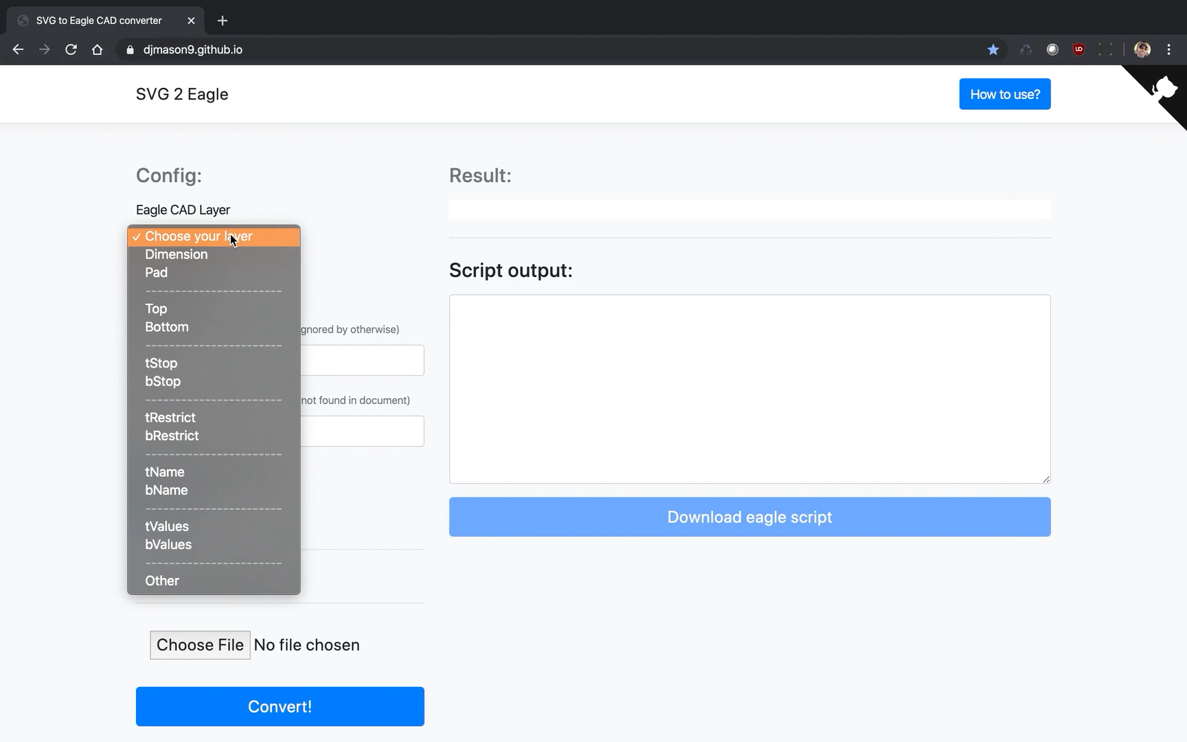
Simply pick the layer type choose the correct file to import and press the convert button. You can even assign a signal name to the layer if you want (such as GNG). This will output the script that you can either copy and paste or download to your computer (download is recommended for stability)
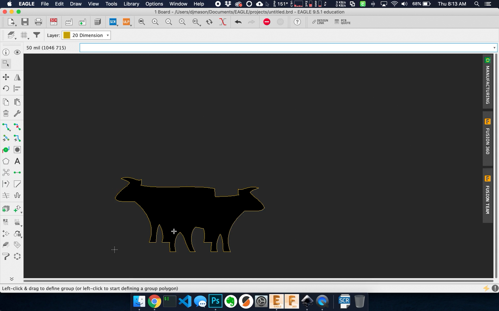
Step Four Eagle Cad
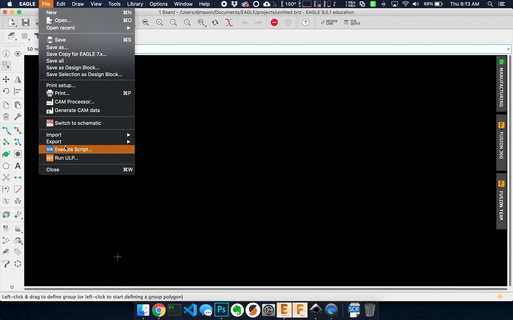
This is where we import our newly created script files into Cad. (Menu Item: File > Execute Script ...)
You should now see your custom shapes start to appear.